Shaping the Future of Semiconductor Manufacturing with Breakthrough Materials

Unlock the next era of semiconductor advanced packaging efficiency with Terefilm® photopolymer

What is Terefilm®?

Terefilm® photopolymer is an innovative materials solution to key semiconductor industry challenges including precision mass transfer, high-resolution photolithography, and temporary bonding-debonding.

The unique balance of precise patternability, clean decomposition, and low activation energy make Terefilm® the clear choice for high throughput semiconductor applications requiring precise control and stringent cleanliness.

How does it work?

Terefilm® offers thermal stability up to ~180 °C prior to UV exposure, allowing for integration into manufacturing process flows with elevated temperature steps. With application of low energy UV irradiation, the decomposition temperature is decreased by more than 100 °C, substantially lowering the energy required for vaporization.  The decomposition can be assisted by acid catalysis using a photoacid generator, very similar to the ones which have been widely used in photoresists for many years. 

Unlike chemically-related photoresists in which minutes or hours may elapse between the exposure of a material and its development, our reaction takes place on a sub-millisecond timescale and results in complete vaporization of the activated region into all gaseous products.

This residue-free transition from a glassy polycarbonate into a gas is what gives Terefilm® its unique range of applications.


Key Benefit: Low Activation Energy

The performance of Terefilm® relies on bringing volatile decomposition products to sufficient temperatures to vaporize. This vaporization occurs at ~60 °C, enabling market-leading low energy input (or fluence) for activation. This means lower power usage, longer lifetimes of optical components, and larger area processing. Specific fluence requirements are dependent on laser pulse-width, since the time over which the energy is applied is directly related to the maximum temperature the material will reach.

Terefilm® activates at energies below the ablation threshold of most mask materials, opening up a world of applications where selective release of components is required (MicroLED mass transfer, for example).  

By lowering the cost and extending the serviceable life of both lasers and optics in LIFT systems, production tools taking advantage of Terefilm® deliver a lower Cost of Ownership (COO) than systems requiring material ablation.


Key Benefit: Clean Decomposition

Materials designed to decompose under high energy light application typically undergo ablation, leaving behind significant amounts of carbon residue, and necessitating energy- and materials- intensive cleaning processes to remove particles detrimental to device performance.

Terefilm® is the only photopolymer solution on the market designed to vaporize entirely upon activation, eliminating the need for downstream cleaning steps and ensuring component cleanliness.

Key Benefit: Precise Patterning

Uncontrolled material decomposition, or ablation, cannot provide well-defined spatial and temporal control. For precision placement applications, mass imbalances detrimentally skew component trajectories.

For laser transfers, low fluences make photomasking possible, allowing for selective die release and pitch conversion as well as massive throughput benefits: thousands or millions of components can be transferred with a single nanosecond laser pulse.

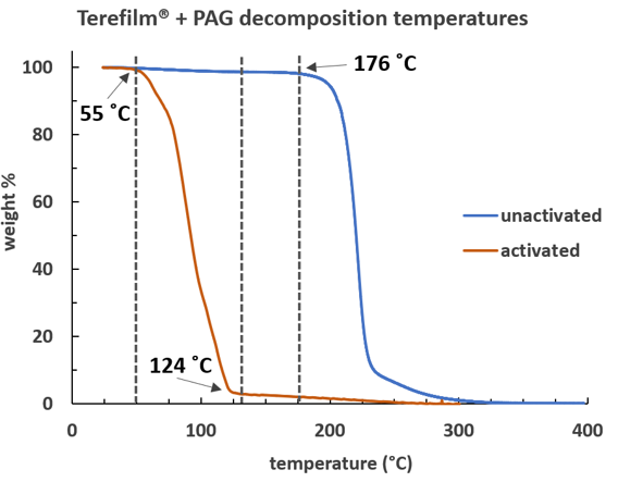
Terefilm® is the only transfer material specifically engineered for Laser Induced Forward Transfer (LIFT) of small, thin, and fragile components.  This is achieved through a uniquely controlled decomposition pathway which ensures uniform activation and vaporization over targeted areas, so customers can be confident in the reliability and reproducibility of the decomposition behavior, whether for precision component placement, high-resolution patterning, or gentle release of bonded wafers.

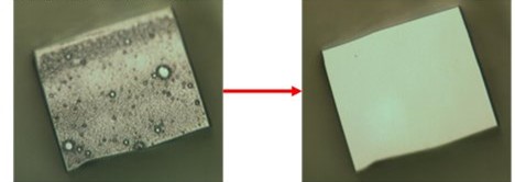
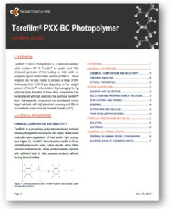
Above: Irradiation of 0.34 µm thick Terefilm® coating using a 50 x 60 µm projection mask and 90 mJ/cm2 to demonstrate activation region. Profile of laser-activated regions show nearly vertical sidewalls, instrumental to selective transfer of components with <1 micron street width with no impact on neighboring dies.

Download a copy of our Material Guide to learn more about Terefilm®

Terefilm Material Guide

Want to learn more about Terefilm® properties, usage guidelines, and whether it might be a good fit for your application?