Build encapsulated circuits without PCBs or substrates

Packaging & Assembly Reinvented

What is SiP?

Future efficiencies in electronics will come from disaggregation of functionality and “Systems in Package”, or SiP This means that many different types of technologies (silicon ICs, analog devices, passives, microelectromechanical sensors, 5G radios and other devices and systems) are put together in novel ways to achieve greater performance and new functionality.

Building these products introduces requirements that cannot be met with the transistor scaling that served so well in the Computer era.  Crystals, antennas, passives, power circuitry, and compute logic are all fabricated from different materials, so they must be integrated at the packaging and assembly level.

Application: Internet of Things

The 3rd Industrial Revolution transformed Business Processes with the introduction of computers, mobility, and the Internet. Manufacturing adapted with the semiconductor age and six decades of continuous improvement.

Now, in the 4th Wave of Industrial Innovation, new advances will transform Everyday Objects by instrumenting the world – the Internet of Things.  Sensors, displays, AI, GPS, and 5G technology combine to give us smart thermostats, watches, doorbells, signage, cars, appliances, glasses . . . even windows.  And the best is yet to come.  

With all of these devices interconnected through cloud services, data can be aggregated and IoT devices can respond intelligently to inputs – autonomously and in real-time.

Application: Health Tech

Smart watches, wristbands, rings, jewelry and patches are just the start of wearable devices designed to monitor and report biological functions. 

While earlier devices were limited to heart rate monitoring and step counting, the near future will see the convergence of the health and fitness category with true medical devices capable of tracking blood pressure, noninvasive glucose monitoring for people with diabetes, ECG recording for heart health, metabolic analysis, and even cognitive functioning,   Leading-edge ingestible sensors take this approach further, relaying information to physicians from within the body.  

These new Health Tech devices will also connect to the emerging IoT infrastructure, providing personalized user feedback and alerts through smartphones and amassing anonymized data from the community for medical research and public health.

0

The Challenge: Complexity and Scale Up

A diverse set of incredibly small components make up these devices.  A Health Tech device, for example, may need stretch and pressure sensors, as well as chemical, optical and biopotential sensors, analog-to-digital converters, memory devices, and CPUs.  Radios and antennas are needed to transmit the data to smart phones or IoT edge devices through Bluetooth, WiFi, or 5G networks.  All of this needs to be locally powered by rechargeable batteries, miniaturized to a wearable or ingestible scale, and encapsulated in a flexible, leak-free and biologically inert material. 

While U.S. households today own from 7 to 15 connected network devices, the potential for Heath Tech and IoT devices can easily rise to hundreds per household, plus industry (Smart Buildings) and municipalities (Smart Cities.) This translates to a manufacturing challenge of producing billions of tiny complex electronic units – a scale that has never been seen before.

Our Solution - New Materials & Design Language for SiP Manufacturing

Due to the wide variety of components required, heterogeneous systems like IoT devices cannot be fabricated using the same semiconductor processes that gave us CPUs and memory.

Building electronics the traditional way – on printed circuit boards (PCBs) connected with metal wires and traces – is not ideal for IoT and MedTech.  Each component on a PCB is individually attached to a lead frame and encapsulated, resulting in vast amounts of unused board space, signal integrity degradation, and wasted power. It is also difficult to achieve the desired miniaturization and flexibility with PCBs.

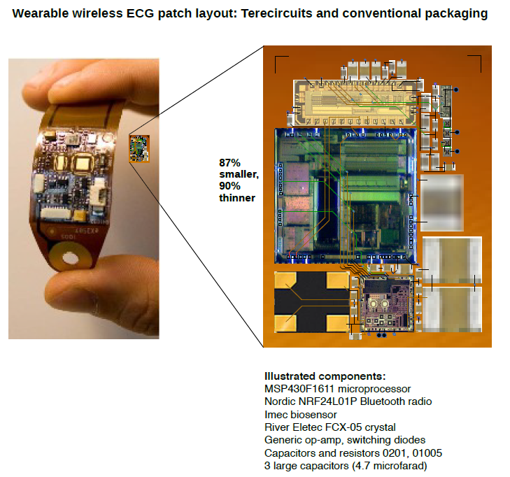
Terecircuits’ unique placement technology allows singulated die and other components to be placed within microns of each other then encapsulated using our flexible, low-viscosity fill material.  For flexibility, the components can be thinned to 25-150 microns.  Interconnects are formed with the same metal structures that are used in the ICs themselves, eliminating solder which is the dominant source of failure in PCBs.    

The final product is an encapsulated SiP device that is smaller, thinner, flexible, and less expensive to produce.  And, by leveraging the ability of our photo-polymer mass transfer process to pick up and place hundreds of components simultaneously, it is possible to fabricate hundreds of identical SiP assemblies in parallel.