We cross-develop new manufacturing processes alongside new materials

Meeting today’s most demanding challenges requires more that incremental improvements in materials

Chemistry - but much more

Our materials are designed to support a system handling and packaging approach which meets today’s needs for unprecedented assembly speed, thinness, miniaturization, and low cost, with superior yield and reliability.  Often this means envisioning new ways to improve or re-invent manufacturing processes.  

Terecircuits’ expertise goes beyond chemistry and material science to encompass lithography, circuit design, process engineering, design for manufacturing, and mechatronics.  That’s why many of our materials are unique in the market, and support processes that outperform conventional approaches.  We’re interested in solving the big problems that others struggle with, like MicroLED panel assembly and SiP packaging for IoT devices.

Challenge: Placing small components

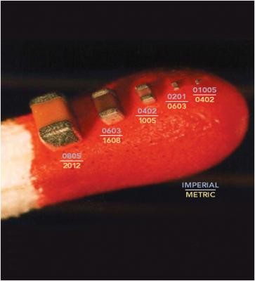
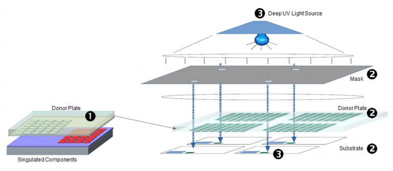
Assembling circuits is increasingly challenging as components continue to shrink.  In extreme cases, like MicroLEDs, individual devices can be from 2-40 microns in diameter, or about the size of a blood cell.  At this scale, Van der Waals and electrostatic forces are more powerful than gravity.  That means once picked up, components are difficult to release. 

Terecircuits’ component transfer process uses a very thin layer (1 µm or less) of our photo-polymer on a transparent plate to hold the chips.  In this “Transfer” state, our novel polymer has a high bonding strength and can sustain elevated temperature processing in the range of 200-300º C.  

In the “Release” state, the polymer undergoes clean decomposition when activated by deep UV irradiation.  The chips will be placed with uniform pressure and will be perfectly aligned on the target substrate. 

Challenge: Speed and accuracy

Conventional pick-and-place tools, assuming they can even handle components at that scale, need to slow down to accommodate the mechanical settling time needed for placement accuracy.  Because pick-and-place is a serial process that handles components one at a time, throughput goes down with decreasing component geometry.  

Using our process,  multiple components can be simultaneously placed on a surface, limited only by the size of the mechanical fixture for the substrates.  Since Terecircuits can place thousands of components at once, throughput actually increases with smaller geometry components, achieving greater than 400K Units Per Hour (UPH) with sub-micron placement accuracy.

Challenge: Cost

Typically, pick and place equipment, including a full complement of feeders, constitute about 50% of the total capital investment required for a medium volume circuit assembly line and 28% of the capital investment for the semiconductor assembly process.  In the display industry, the depreciation of the specialized tools used in the fabrication of OLED displays are the single largest contributor to panel cost.

By using a photo-polymer transfer process and our adhesive polymer in conjunction with a fine granular alignment system, these tools could be replaced with simpler and less expensive stage motion tools adapted from lithography, saving costs while enabling next gen products.

Process Example: Photo-polymer Mass Transfer

The Terecircuits process can achieve sub-micron placement accuracy and fabricate entire systems from subunits (a SiP or MicroLED display panel, for example), replacing a process typically done with pick-and-place machines.  

The process is illustrated here:  (1) A transparent donor plate coated with sticky polymer picks up any number of components; (2) A fine granular positioning tool aligns the stack of mask, donor plate, and substrate; and (3) Light activation selectively releases the components, precisely placing them on the substrate