All exponential processes eventually end.
Moore's law is no exception.

The Challenge

An End to Transistor Scaling?

The Computer Era: Six Decades of Transistor Scaling

From this...
(12 transistors, circa 1960)

12 Transistor Radio (Transparent)

To this.
(4.3 Billion transistors, 2020)

apple-iphone-x-00-gray-600x600-hero

In the early days of electronics, individual transistors and passive components were placed on printed circuit boards and soldered in place. The integrated circuit allowed entire functional circuits composed of multiple transistors and passive components to be fabricated at once, limited only by lithographic and etching resolution.  Moore’s Law refers to the process improvements that have delivered a doubling of transistor density every two years. 

Since the cost of fabricating transistors on one square centimeter of silicon has remained extraordinarily close to constant over six decades of Moore’s Law, the Computer era has consistently delivered smaller, cheaper transistors and more sophisticated “chips” year after year.  We have far more computing power in our pockets today than occupied an entire rack in 1980.

All exponential growth processes end eventually, and Moore’s Law is no exception.  The physics of patterning systems limits the size of the system that can be made in one integrated parallel process, and process compatibility limits the type of materials.  In fact, the products of Industry 4.0 often cannot benefit from shrinking transistors because they are not purely transistor-based.

Moore's Law: "Transistor Density Doubles Every 2 Years"

SiP: Extending the Trend with Advanced Packaging and Assembly

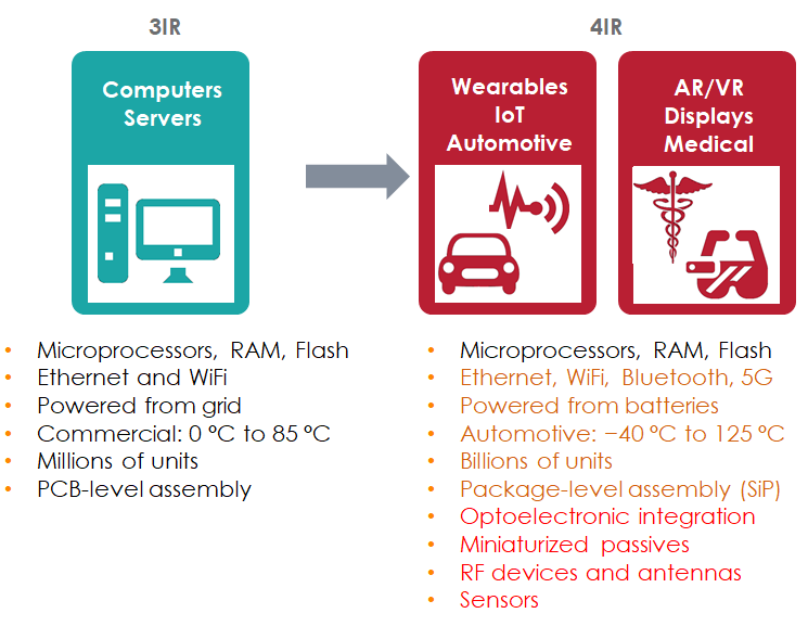
The products that are currently being worked on are amazing, from phones that can be folded, to nanobots that can gather diagnostic data from within the human body, to voice activated personal assistants worn like a ring, to transparent near eye AR displays that can be embedded in the lenses of eyeglasses and powered by new battery technology hidden in the frames. 

Building these products introduces requirements that cannot be met with the transistor scaling that served so well in the Computer era.  To deliver these products relies on solving new manufacturing challenges – low cost transparent and flexible displays with high pixel density, embedded sensors, extreme miniaturization, and lighter weight, lower power circuitry.  And, in the Internet of Things era, new manufacturing processes will need to scale up to produce Billions of units with good yields.

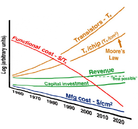
Today, innovation in microelectronics is centered on Packaging, and specifically heterogeneous packaging.  As Moore’s Law scaling approaches physical limitations, future efficiencies in electronics will come from disaggregation of functionality and “Systems in Package”, or SiP This means that many different types of technologies (silicon ICs – digital or analog, compound semiconductor ICs and light emitters and receivers, microelectromechanical sensors, and other devices and systems) are put together in novel ways to achieve greater performance and new functionality.

THE SOLUTION

SiP
"System in Package"